Semiconductor and Devices Formulas
Quickly grab the opportunity and utilize the Semiconductor and Devices Formulas list and get a good grip on the concept. Avail the Semiconductor and Devices Formula Sheet and learn the concept in a simple manner. We have covered everything right from Conductors, Insulators, Semiconductors, P-Type & N-Type Semiconductors, etc. Avail the Formulae List and try to apply them during your homework or assignments. For more help on related concepts check out Physics Formulas and learn the logic behind them.
Cheat Sheet for Semiconductor and Devices
1. Energy bands in solids
- Valence band,
- Conduction band and
- Forbidden energy band
2. Conductors
- Conductors do not have a forbidden energy gap between valence and conduction bands.
- Conductivity is very high between 106 to 108 mho/m.
- Resistivity is between 10-8 to 10-6 ohm-m.
- Temperature coefficient of resistance is positive.
- Current is due to flow of free electrons.
- All metals are conductors.
3. Insulators
- The forbidden energy gap between valence and conduction band is very large (~ 5 eV) as compared to thermal energy (~ 0.025 eV).
- Conductivity is negligible, between 10-7 to 10-16 mho/m.
- Resistivity is very high, between 107 to 1016 ohm-m.
- Temperature coefficient of resistance is negative.
- Examples are diamond, wood, glass etc.
4. Semiconductors
- The forbidden energy gap between valence and conduction bands is about 1 eV. In Ge it is 0.78 eV and in Si it is 1.1 eV. These are fourth group elements.
- Conductivity is between 10-3 to 101 mho/m.
- Resistivity is between 10-1 to 103 ohm-m.
- Temperature coefficient of resistance is negative because the number of charge carriers increases with increase of temperature.
- The flow of current is due to electrons as well as holes.
5. Intrinsic semiconductors
- These are pure semiconductors as Ge, Si
- These behave as insulators at absolute zero.
- The covalent bonds are broken by thermal energy creating free electrons and holes.
- The number of electrons in conduction band is equal to number of holes in valence band.
- Current density J = nq\(\left(\bar{v}_{e}+\bar{v}_{h}\right)\)
- Conductivity σ = \(\frac{\mathrm{J}}{\mathrm{E}}\) = nq(µe + µh)
- The number density of electrons in conduction band at T K is
n = AT3/2e-ΔEg/2kT
6. Extrinsic semiconductors
- These are doped by impurities. The impurities are either of fifth or third group.
- When impurity is of fifth group (P, Sb, As, Bi etc) N-type semiconductor is formed.
- When impurity is of third group (B, Al, In etc.) P- type semiconductor is formed.
7. N-type semiconductors
- Majority charge carries are electrons.
- J Γëê nq \(\overline{\mathbf{v}}_{e}\)
- a Γëê nq┬╡e
8. P-type semiconductors
- Majority charge carries are holes.
- J Γëê pq\(\overline{\mathbf{v}}_{h}\)
- a Γëê pq┬╡h
9. P-N junction diode
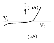
- Obtained by joining P-type and N-type; semiconductors at atomic level.
- There is a layer at the junction devoid of free charge carriers, called depletion layer.
- A potential barrier is developed at the junction.
- In forward bias the barrier height decreases and current increases exponentially. The dynamic resistance is low (~100 ohm).
- In reverse bias condition the barrier height increases. The current is in opposite direction and almost constant (saturation current ~ ┬╡A). The dynamic resistance is high (~ 106 ohm).
- The I-V relation is I = I0 (eqV/kT – 1)
10. Zener diode
- In the reverse bias condition if the voltage is increased beyond a certain limit the current increases abruptly.
- This process is due to avalanche breakdown.
- The critical voltage is called Zener voltage
- Zener diodes are used as voltage regulators.
11. Rectifier
(i) The process of conversions of alternating voltage into direct voltage is ; called rectification and the device is called rectifier.
(ii) Half wave rectifier: It uses half of the input wave. The output current and j voltage is pulsating and its frequency is same as frequency of input voltage.
Idc = \(\frac{I_{0}}{\pi}\), Irms = \(\frac{I_{0}}{2}\), Ripple factor r = 1.21
Efficiency ╬╖ = \(\frac{40.6}{1+r_{p} / R_{L}}\) %, ╬╖max = 40.6 %
(iii) Full wave rectifier
(a) It rectifiers the full wave
(b) Two identical diodes are used. The output current and voltage are pulsating whose frequency is double the frequency of input alternating voltage.
(c) Idc = \(\frac{2 \mathrm{I}_{0}}{\pi}\), Irms = \(\frac{I_{0}}{\sqrt{2}}\), Ripple factor r = 0.48
Efficiency ╬╖ = \(\frac{81.2}{1+r_{p} / R_{L}}\) %, ╬╖max = 81.2 %
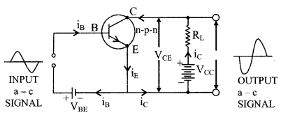
12. Transistor
(i) Drives current from low resistance at input to a high resistance at output. It is a current controlled device.
(ii) Two types are NPN and PNP
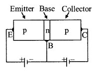
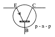
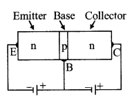
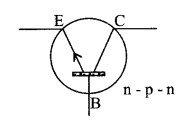
(iii) The end parts i.e. emitter and collector are of same kind of semiconductor while the central part base is of opposite kind.
(iv) The emitter-base junctions is always forward biased while collector-base junction is reverse biased.
(v) IE = IB + IC. IB << IC therefore IC Γëê IE
(vi) The input resistance is low while the output resistance is very high.
13. Configurations of transistor
Three configurations exists
- Common base
- Common emitter
- Common collector
14. Current gain
(i) In common base configuration current gain
╬▒ = \(\frac{\Delta \mathrm{I}_{\mathrm{C}}}{\Delta \mathrm{I}_{\mathrm{E}}}\) Γëê 1 (slightly less than 1)
(ii) In common emitter configuration
current gain ╬▓ \(\frac{\Delta \mathrm{I}_{\mathrm{C}}}{\Delta \mathrm{I}_{\mathrm{B}}}\) >> 1
(iii) ╬▒ = \(\frac{\beta}{1+\beta}\)
15. Transistor amplifier
(i) Usually common base and common emitter configurations are used.
(ii) Common base & common collector configuration create no phase difference but common emitter configurations create π phase difference between input & output.
(iii) For input resistance Ri and load resistance RL
Current gain Ai = ╬▒ or ╬▓ according to configuration.
Voltage gain Av = current gain × resistance gain
= (α or β) × \(\frac{R_{L}}{R_{i}}\)
Power gain Ap = current gain × voltage gain
= (α or β)2 × \(\frac{R_{L}}{R_{i}}\)
Have a glance at the go-to place for any kind of formulae pertaining to various physics concepts under one roof at Physicscalc.Com a genuine portal.